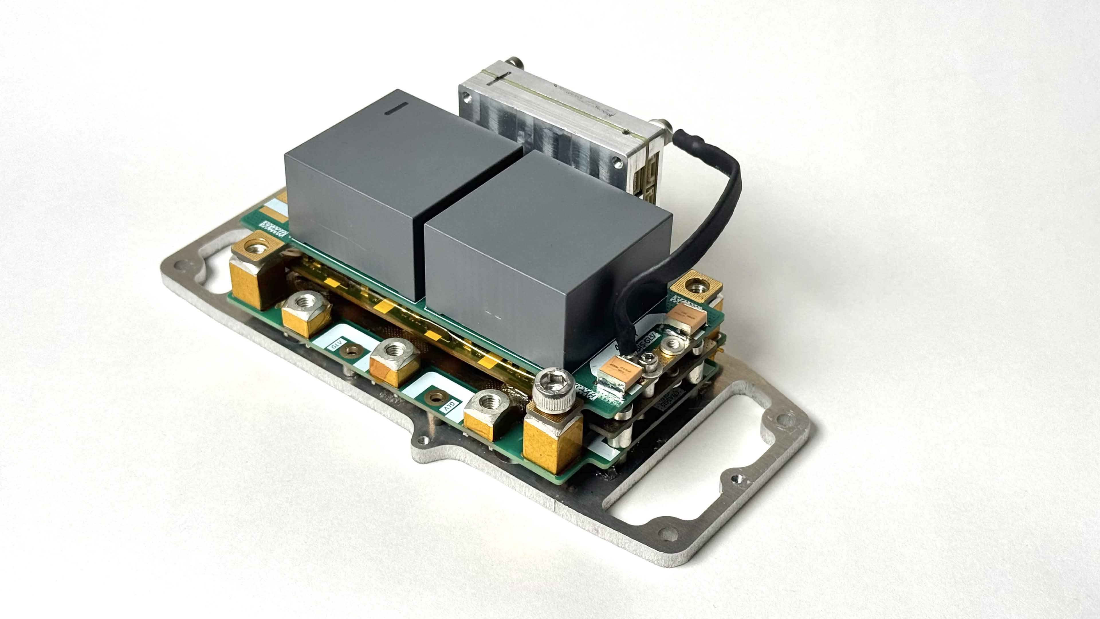
High Efficiency PMSM Inverter for EV Application | https://github.com/liongma/Inverter
Co-Optimization of a 3-Phase, 50 kW, 600 V Power-Dense SiC VSI for PMSM Drive
Liong Ma Massachusetts Institute of Technology liongma@mit.edu
1. Introduction
Electric vehicles (EVs) are advancing quickly to meet decarbonization goals, driven by better batteries, faster charging, and higher-performance motors. At the heart of every EV is the traction inverter — the power electronics that converts battery DC power into the AC power needed to drive the motor. Because EVs are judged on range, performance, and cost, traction inverters are under constant pressure to become more efficient and more power-dense.
Most production traction inverters today use silicon IGBTs because they are cheap and reliable, reaching power densities around 50 kW/L. However, wide-bandgap (WBG) semiconductors — silicon carbide (SiC) and gallium nitride (GaN) — can switch faster and pack more power into less volume, potentially beating IGBTs on energy density and even cost. The tradeoff is that WBG devices bring new challenges: more EMI, tougher thermal management, and open reliability questions. A systematic way to optimize WBG-based inverters for cost, density, and performance — without sacrificing reliability — is needed before WBG technology can be widely adopted in EV drivetrains.
The Formula Student/FSAE competition gives university teams a chance to try state-of-the-art technology before it reaches industry. This project develops, builds, and tests a WBG-based traction inverter for the MIT FSAE car to demonstrate what WBG technology can do in an EV drivetrain.
A central challenge in building a power-dense inverter is that its design choices are all coupled — changing one parameter (like switching frequency) shifts the best choice for several others (like capacitor size or heat sink size). This calls for a numerical co-optimization approach. Prior work modeled the power module, DC-link capacitor, and cooling system together to define a system-level design space for optimization. This paper extends that framework by adding cost-effectiveness and comparing multiple power-electronics architectures and semiconductor types.
The approach has three stages:
- Build a loss model for the inverter across different topologies and switching devices, and select device candidates.
- Relate switching frequency to DC-link capacitor volume and heat sink thermal resistance.
- Project the cost-effectiveness of candidate devices to narrow the design space and find the best operating points for efficiency, power density, and cost.
2. Design Overview
The target motor is a permanent magnet synchronous motor (PMSM) from AMK.
Table 1 — DD5-14-10-POW Motor Specifications
| Parameter | Value |
|---|---|
| Mass | 3.55 kg |
| Rated Torque | 9.8 Nm |
| Rated Continuous Power | 12.3 kW |
| Rated Speed | 12,000 rpm |
| Maximum Speed | 20,000 rpm |
| Rated Voltage | 350 V RMS |
| Rated Current | 41 A RMS |
| Maximum Current (1.24 s) | 100 A RMS |
| Flux Linkage | 0.028 Wb |
| Pole Pairs | 5 |
Several circuit topologies can drive a PMSM: multilevel converters, voltage source inverters (VSIs), and current source inverters (CSIs). CSIs need bulky external magnetics that don’t scale well at kW power levels, so they’re a poor fit for a volume-optimized design. The voltage source inverter (VSI) is chosen instead — it’s simpler, easier to control, and cheaper. (Other topologies may be better for larger, higher-power designs.)
A standard VSI is built from switching transistors (FETs), decoupling capacitors, and DC-link capacitors. It works by switching each motor phase’s voltage on and off in sync with the rotor angle. The switches operate in hard-switching mode, which limits how fast they can switch due to switching losses. DC-link capacitors filter the input to reduce voltage ripple (and therefore motor torque ripple); an additional input filter is often added to cut input current ripple, which would otherwise cause transmission losses and conducted EMI.
This paper’s contribution is a device-level co-optimization of a SiC-based converter using numerical modeling. The board is then designed and tested on a regenerative dynamometer under full voltage and current load, and the controls are tuned for stable, high-performance operation at high motor speed.
3. Loss Modeling
The power loss model drives both the cooling system design and the achievable efficiency. Since transistor power dissipation is limited by the thermal performance of the package and thermal interface material, losses also constrain which architectures are even feasible.
3.1 Design Requirements
The target system is a three-phase PMSM driven by a two-level totem-pole inverter:
- DC-bus voltage: $V_{dc} = 600\text{ V}$
- Maximum output power: $P_o = 50\text{ kW}$
Each phase’s output power relates to output voltage and current:
$$ P_o = \sqrt{3}\,V_{ac}\,I_{rms} = \sqrt{3}\,V_{ac}\,\frac{I_m}{\sqrt{2}} $$where $V_{ac}$ is the RMS line-to-line output voltage, $I_{rms}$ is the RMS phase current, and $I_m$ is the peak phase current.
Under classical sinusoidal PWM (SPWM), with modulation index $m$:
$$ I_m = \frac{\sqrt{6}\,P_o}{3m\,V_{ac}} = \frac{4P_o}{3m\,V_{dc}} $$3.2 Conduction Losses
In each phase-leg, the high-side and low-side switches split conduction losses equally over a full electrical cycle (by symmetry). Dead-time effects are also accounted for and subtracted from the base conduction-loss estimate:
$$ P_{con,H} = \frac{I_m^2}{n^2}\left(\frac{1}{8} + \frac{m\cos\phi}{3\pi}\right) R_{ds,on} $$$$ P_{con,L} = \frac{I_m^2}{n^2}\left(\frac{1}{8} - \frac{m\cos\phi}{3\pi}\right) R_{ds,on} $$where $n$ is the number of parallel devices, $\phi$ is the power factor angle, and $R_{ds,on}$ is on-state resistance.
Dead-time conduction through the body diode adds:
$$ P_{con,dt} = t_{dt}\,f_{sw}\left(\frac{\pi}{2}\,R_F\,\frac{I_m^2}{n^2} + 2V_F\,\frac{I_m}{n}\right) $$with an overlap correction:
$$ P_{con,red} = \frac{1}{2}\,\frac{I_m^2}{n^2}\,R_{ds,on}\,t_{dt}\,f_{sw} $$Total three-phase conduction loss:
$$ P_{con} = 3n\left(P_{con,H} + P_{con,L} + P_{con,dt} - P_{con,red}\right) $$3.3 Switching Losses
Turn-on/turn-off losses are found from per-event energies $E_{on}$, $E_{off}$ measured at rated test conditions ($V_n$, $I_n$) and scaled to the operating point:
$$ P_{sw,on} = E_{on}\,f_{sw}\,\frac{V_{dc}\,I_m}{\pi\,n\,V_n\,I_n} \qquad P_{sw,off} = E_{off}\,f_{sw}\,\frac{V_{dc}\,I_m}{\pi\,n\,V_n\,I_n} $$Reverse-recovery losses (relevant for Si IGBT and Si/SiC body diodes):
$$ P_{rec} = E_{rec}\,f_{sw}\,\frac{V_{dc}\,I_m}{\pi\,n\,V_n\,I_n} $$GaN devices typically avoid reverse-recovery loss unless a cascode or external-diode architecture is used.
Output-capacitance loss, from switched charge $Q_{oss}$:
$$ P_{oss} = V_{dc}\,Q_{oss}\,f_{sw} $$Gate-drive loss:
$$ P_g = (V_C - V_E)\,Q_{g,tot}\,f_{sw} $$where $Q_{g,tot}$ is total gate charge and $V_C$, $V_E$ are turn-on/turn-off gate voltages.
Total switching loss per phase-leg:
$$ P_{sw} = n\left(P_{sw,on} + P_{sw,off} + P_{rec} + P_{oss} + P_g\right) $$3.4 Combined Inverter Losses
Each phase-leg’s total loss:
$$ P_{loss,ph} = P_{con} + 2P_{sw} $$Adding DC-link capacitor ESR loss:
$$ P_{loss,dc} = I_{c,rms}^2\cdot ESR(f) $$plus resistive losses in the PCB copper (limited to 2 oz copper in this manufacturing process), the total three-phase inverter loss is:
$$ P_{loss,inv} = 3P_{loss,ph} + P_{loss,dc} = 3P_{con} + 6P_{sw} + P_{loss,dc} $$4. Volume Modeling
Inverter volume is dominated by three things: the FET power stage, the DC-link capacitor, and the cooling solution. This total volume determines power density and is the second major axis of the optimization. Power-stage volume is treated as roughly constant (transistors, gate-drive circuitry, compute, and auxiliary electronics); capacitor and thermal sizing are modeled from empirical data.
4.1 Capacitor Volume
The DC-link capacitor decouples the switching current ripple of the FETs from the DC-link voltage. It must be large enough to keep voltage ripple below a target level while also handling the RMS ripple current.
$$ I_{Cdc,RMS} = \hat{I}\sqrt{M\left(\frac{\sqrt{3}}{4\pi} + \cos^2\phi\left(\frac{\sqrt{3}}{\pi} - \frac{9M}{16}\right)\right)} $$$$ C_{Cdc,RMS} = \frac{I_{Cdc,RMS}}{5\,f_{sw}\,C} $$$$ \Delta V_{dc,pp} = \frac{\Delta Q}{C_v} = \frac{I_m}{C_v\,f_{sw}}\,q(m,\phi) $$This required capacitance maps to a physical volume that scales with voltage. Film capacitors are used for bulk capacitance because of their performance, reliability, and cost.
The capacitance–ripple-current relationship:
$$ C_i = k_{C1} I_{c,rms} + k_{C2} $$and the volume–capacitance relationship:
$$ v_c = (k_{V1} C_{dc} + k_{V2})\, V_n $$where $v_c$ is capacitor volume and $k_{V1}$, $k_{V2}$ are empirical coefficients (Table 2).
Table 2 — Empirical Capacitor Sizing Coefficients
| Capacitor | $k_{C1}$ (µF/A) | $k_{C2}$ (µF) | $k_{V1}$ (mm³/V·µF) | $k_{V2}$ (mm³/V) |
|---|---|---|---|---|
| Kemet | 3.0 | −17.8 | 1.8 | 12.2 |
| TDK | 2.4 | −10.1 | 2.0 | 17.3 |
| Vishay | 3.3 | −24.3 | 2.4 | 16.4 |
Using these relationships, both the ripple-voltage-driven and ripple-current-driven capacitance requirements are computed, and the larger one sets the final capacitor volume.
4.2 Heat Sink Volume
Liquid cooling keeps junction temperature below the device’s maximum rating. In practice, some margin is needed to avoid thermal runaway or uneven heating, so a more conservative case-temperature limit of 120 °C is used.
The thermal path from FET junction to ambient has three parts: the device’s junction-to-case resistance ($Rth_{jc}$, from the datasheet), the thermal interface material (TIM) resistance, and the heat sink resistance. A high-performance silicone TIM at 0.5 mm thickness achieves about 1 W/K, so the heat sink resistance is the limiting factor. Different cooling solutions’ thermal resistances are compared to determine the cooling volume needed to hit the target thermal resistance at each switching frequency.
5. Power Transistor Selection
Transistor choice strongly shapes the loss model and the optimum operating point. The three main technologies compared are IGBT, SiC, and GaN.
The motor’s fundamental electrical frequency:
$$ \omega_{emax} = RPM \cdot \frac{2\pi}{60} \cdot N_{pp} $$For this motor, that’s 1.7 kHz. A common rule of thumb sets the PWM switching frequency at 10× the fundamental, or about 17 kHz, for robust control.
The minimum DC-link voltage needed to reach the motor’s top speed under space-vector PWM (max modulation index $m_{max} = 1/\sqrt{3} \approx 0.577$) is:
$$ V_{dc} \geq \sqrt{3}\, N_{pp}\, \omega_{emax}\, \psi_e $$DC voltage must stay above 400 V at all operating points so the motor is never speed-limited, so the battery is sized to 600 V (with $V_{min,SOC} > 400$ V). This means devices need a DC withstand voltage above 600 V — ideally with more margin to reduce electro-migration and drain wear-out.
Silicon IGBTs have the best static (conduction) loss characteristics but WBG devices (SiC, GaN) have much better dynamic (switching) loss characteristics. Comparing candidate state-of-the-art devices: SiC keeps losses very low even at high switching frequency, beating IGBT clearly and beating GaN on conduction loss. The chosen device is the SCT011HU75 (ST Microelectronics).
Table 3 — SCT011HU75 FET Specifications
| Parameter | Value | Parameter | Value |
|---|---|---|---|
| $V_{DS}$ | 750 V | $C_{oss}$ | 300 pF |
| $V_{GS}$ | −5 to 18 V | $C_{iss}$ | 3860 pF |
| $T_J$ | −55 to 175 °C | $R_G$ | 1.2 Ω |
| $R_{thJC}$ | 0.23 °C/W | $V_{SD}$ | 2.6 V |
| $R_{DS}$ | 14.2 mΩ | $Q_G$ | 154 nC |
6. Driving Parameter Identification
Switching frequency ties together efficiency, transient response, and power density. Higher switching frequency improves transient response and shrinks passive components (boosting power density), but increases harmonic distortion and lowers efficiency. If efficiency drops too much, the inverter needs more cooling volume, which can reduce power density — hence the need to co-optimize switching frequency.
Two figures of merit (FOMs) guide this study:
- Gravimetric power density of each inverter module (kW/kg)
- Overall inverter efficiency (%)
The efficiency model (from Section 3) is swept over input voltage and switching frequency to build efficiency-frequency (“rainbow”) plots. Combined with the volume-frequency relationship for the DC-link capacitor and the thermal-resistance-frequency constraint for the heat sink, this produces a joint efficiency/power-density model used to find Pareto-optimal design points.
Key results:
- Efficiency is highest below 20 kHz switching frequency and drops off quickly above that.
- Power density is very low at low switching frequency and low output power, but rises sharply and peaks around 20 kHz.
- A “knee point” near 15 kHz marks where further frequency increases give diminishing power-density gains for a steep efficiency cost.
- The theoretical maximum power density, assuming 100% volume utilization, is 170 kW/L.
- Plotting efficiency against power density reveals a Pareto frontier with a knee point — this identifies the optimal switching frequency given the design constraints.
7. Gate Driver
7.1 Driver Architecture
SiC gate drivers are most commonly isolated gate drivers, providing high-voltage isolation from the low-voltage PWM signal. Benefits include a small footprint, integrated dead-time, and shoot-through protection. They do require an isolated bias supply capable of powering both high- and low-side gate drives across the isolation barrier — necessary both between high/low sides (due to voltage potential difference) and between each side and the low-voltage controller (for safety).
Three architectures for distributing power to a high-voltage totem-pole inverter’s gate drivers:
- Fully Distributed — 6 separate isolated bias supplies (one per high/low side per phase). Most robust (a single supply failure doesn’t disable other phases) and best decoupled, but bulky due to many small magnetics.
- Centralized — one power supply distributes isolated power to all phases. Can be much smaller (one larger transformer) but more prone to EMI and single-point failure.
- Semi-Distributed — one power module per phase, supplying both its high- and low-side circuitry. A compromise: fewer modules than fully distributed (smaller footprint) while keeping good decoupling and EMI performance.
Semi-distributed is selected for its balance of small footprint and proximity to the power module.
7.2 Driver Selection
The gate driver must meet these requirements:
- Common Mode Transient Immunity (CMTI)
- High-voltage isolation
- Sufficient gate drive voltage
- Adequate sink/source current
- Fast signal propagation
- Shoot-through protection
FET rise/fall time is normally tuned experimentally based on allowable EMI and overshoot; an initial estimate of 20 ns is used here, based on a realistic commutation loop inductance and half-bridge output capacitance:
$$ \left|\frac{dv}{dt}\right| \approx \frac{\Delta V_{DC}}{\Delta T_{rise}} $$For a 600 V bus, this gives $dv/dt \approx 30$ V/ns — the gate driver’s isolation must withstand this transient at every switching event. For automotive systems above 400 V, reinforced isolation is typically required for safety.
Required sink/source current can be estimated as:
$$ I_{Source} \approx \frac{Q_{iss}}{\Delta T_{rise}} \qquad I_{Sink} \approx \frac{Q_{iss}}{\Delta T_{fall}} $$Propagation skew between high- and low-side drivers must be well below the dead-time to avoid shoot-through. Protection features for shoot-through, over-current, over-temperature, and desaturation are also evaluated for effectiveness and footprint.
Chosen gate driver: UCC21550, which meets the CMTI, isolation, drive-current, and dead-time-adjustability requirements.
7.3 Key Component Selection
The bootstrap capacitor is sized first — roughly 50× the gate capacitance is a common rule of thumb, to account for voltage variation and derating. A 1 µF bootstrap capacitor is chosen.
A series bootstrap diode is needed with a reverse breakdown voltage well above $V_{DC}$, low reverse-bias leakage, and fast reverse recovery so it doesn’t drain the bootstrap capacitor.
A bootstrap resistor limits electrical stress and overheating on the capacitor; its value is chosen so the RC time constant stays well below the half-bridge’s switching period.
8. Current Transducer
Closed-loop motor control and over-current protection both need fast, accurate phase-current measurement. Three common sensing options:
- Shunt resistors + isolated amplifier — smallest and cheapest, but needs isolation across the HV boundary and is prone to noise coupling.
- Closed-loop Hall-effect sensors — inherently isolated, so potentially smaller footprint, but limited bandwidth and accuracy.
- Fluxgate sensors — best accuracy and bandwidth, but too big and expensive for a volume-optimized design.
For a shunt-based sensor, sensed voltage is proportional to phase current:
$$ V_{sense} = I_{phase}\, R_{shunt} $$and the amplified ADC input is:
$$ V_{out} = G(I_{phase}\, R_{shunt}) + V_{ref} $$where $G$ is amplifier gain and $V_{ref}$ is the bias offset needed to represent bidirectional current on a single-supply ADC.
A shunt’s power dissipation is:
$$ P_{diss} = I_{phase}^2\, R_{shunt} $$Since dissipation is thermally limited (typically ~2 W for this application), the shunt’s output voltage — and thus its SNR — is inherently low.
Hall-effect sensors are also noise-sensitive, but because the amplifier sits inside the device, the loop area for noise injection is much smaller. Their main downside is phase delay from limited bandwidth.
Amplifier bandwidth and propagation delay must be fast relative to the switching period to support both the control loop and over-current shutdown:
$$ t_{d,sense} \ll \frac{0.05}{f_{sw}} $$Because the current sensor sits on a high-dv/dt node, common-mode noise can easily cause offset or gain errors. The TMCS1126 is chosen for its high bandwidth and strong noise rejection via differential sensing.
Over-current protection uses a hardware comparator trip, independent of the control microcontroller, so a fault can shut down the gate drivers even if the firmware current loop stalls. The trip threshold sits with margin above normal operating current but below the device’s repetitive peak-current rating.
9. EMI Mitigation
Hard-switched totem-pole inverters generate both differential-mode (DM) and common-mode (CM) EMI. DM noise comes from the di/dt of switched inductive current ripple. CM noise comes mainly from high dv/dt at the switch node coupling through parasitic capacitance to chassis/heat-sink ground.
CM noise current can be approximated by modeling the device-to-chassis parasitic capacitance $C_p$ as an injected current source:
$$ I_{cm} \approx C_p\,\frac{dv}{dt} $$Because WBG devices switch much faster than Si IGBTs, $I_{cm}$ is generally larger for SiC/GaN designs at the same $C_p$ — making CM rejection especially important, since this noise can disrupt the control loop and cause device or system failure.
DM noise is approximated by modeling the device-to-victim parasitic mutual inductance $L_m$ as an injected voltage source:
$$ V_{dm} \approx L_m\,\frac{di}{dt} $$Three complementary mitigation strategies are used:
- Layout — minimizing commutation loop area and switch-node-to-heatsink coupling capacitance directly reduces both switching ringing and injected CM current.
- Filtering — a two-stage DM/CM EMI filter at the DC input attenuates conducted noise to within CISPR 25 limits.
- Shielding and grounding — a low-impedance, single-point chassis ground shrinks the radiated-emission loop area and keeps CM return currents away from sensitive analog/control circuitry.
For the CM filter, the choke inductance $L_{cm}$ and line-to-ground capacitance $C_{cm}$ are chosen so the filter’s corner frequency sits a decade or more below the switching frequency, attenuating the fundamental switching harmonic and its early sidebands:
$$ f_c = \frac{1}{2\pi\sqrt{L_{cm} C_{cm}}}, \qquad f_c \lesssim \frac{f_{sw}}{10} $$Snubber networks could damp the LC ringing seen during switching without slowing the transition too much, but due to high voltage and space constraints, snubbers are not used in this design — they rely on dissipating ringing energy as heat, requiring large, pulse-rated components.
10. Hardware Testing and Validation
Validation proceeds through three stages of increasing electrical stress: low-voltage functional bring-up, switch stress validation, and full-power dynamometer testing.
10.1 Functional Bring-Up
Before applying high voltage, the gate driver, bias supplies, current-sensing chain, and protection circuitry are verified at low voltage. Isolation resistance across each isolation barrier is measured with a hipot tester to confirm it exceeds the datasheet rating, and the high-voltage interlock loop is verified to disable the gate drivers when opened.
10.2 Switch Stress Validation
This stage confirms the theoretical loss and thermal model against real measurements.
Static loss measurement: A high-current power supply verifies static losses and the thermal model. Since a FET’s effective on-resistance depends on junction temperature, threshold voltage, gate voltage, and drain current, the total effective resistance (device + PCB trace) is measured directly:
$$ R_{on} = \frac{V_{PSU}}{I_{PSU}}, \qquad P_{static} = V_{PSU} I_{PSU} $$The resulting temperature rise across the TIM and heat sink gives their measured thermal resistance, for comparison against the modeled value:
$$ R_{th} = \frac{\Delta T}{P_{static}} $$Switching loss measurement: Measured both directly (electrically) and indirectly (thermally). The standard method is double-pulse testing, which uses an inductor to ramp current to a target level before a controlled discharge, producing a predictable switching transition at a known current. Voltage and current across the device are captured during each transition to compute losses:
$$ E_{on,meas} = \int_{t_1}^{t_2} v_{DS}(t)\,i_D(t)\,dt \qquad E_{off,meas} = \int_{t_3}^{t_4} v_{DS}(t)\,i_D(t)\,dt $$This requires a high-bandwidth current probe (e.g., a Rogowski coil or precision differential probe); modifying the phase leg to add probing also introduces extra parasitics that can affect measurement accuracy.
The switch-node ringing captured during switching is used to extract the effective commutation loop inductance $L_{loop}$ from the ringing frequency $f_{ring}$ and device output capacitance $C_{oss}$:
$$ L_{loop} = \frac{1}{(2\pi f_{ring})^2\, C_{oss}} $$This measured inductance feeds back into both the gate-driver sink/source current sizing and the EMI current estimate, closing the loop between layout, switching performance, and conducted emissions.
10.3 Dynamometer Validation
Once switching-cell behavior is characterized, the assembled inverter is mounted to the PMSM on a regenerative dynamometer capable of sinking the motor’s full rated power back to the grid or battery. Efficiency is measured directly from electrical input and mechanical (or regenerated electrical) output power:
$$ \eta = \frac{P_{out}}{P_{in}} \times 100\% $$and swept across the torque-speed plane to build a measured efficiency map for comparison against the modeled efficiency surface.
Throughout dynamometer testing, the over-current trip and high-voltage interlock stay continuously armed, and a documented lockout-tagout procedure is followed whenever the high-voltage bus is energized.
11. Conclusion
This paper presents a loss model and co-optimization methodology for three-phase traction inverters. By capturing conduction, switching, reverse-recovery, output-capacitance, and gate-drive losses in closed form — and linking these to passive-component volume and thermal constraints as functions of switching frequency — the design space can be systematically explored. Adding cost projections further narrows candidate devices toward Pareto-optimal operating points across efficiency, power density, and cost-effectiveness.